
What is PCB Depaneling?
PCB (printed circuit board) depaneling, also called singulation, is the process of removing numerous smaller, individual PCBs from a larger multi-PCB panel produced during manufacturing. The depaneling process was created in order to increase throughput of PCB manufacturing lines as circuit board sizes reduced. At CMS Laser, our depaneling process has the advantage of speed, pin-point accuracy, no tooling cost or wear, no part induced stress, and no cutting oils or other waste.
Demand Driven by Size
As technology continues to evolve, the gadgets we use become more advanced and often decrease in size. This reduced size requires smaller PCBs. With no set standard for PCBs, every board is designed for a specific item. Therefore, the process for depaneling separate boards from a multi-image board is unique. Production factors such as stress, precision and cleanliness are paramount to keeping board defects to a minimum.
Depaneling Methods
PCBs are typically manufactured in large panels containing multiple boards at a time, but can also be produced as single units if need be. The depaneling of PCBs process can be fully automatic, manual, or semi-automatic. There are several methods used, including laser PCB depaneling, within the electronics industry. Let’s examine what they are:
Punching/Die Cutting:
The punching method is the process of singular PCBs being punched out of the panel through the use of a special fixture. The punching fixture has sharp blades on one part and supports on the other. A different die is required for each board and dies must frequently be replaced to maintain sharpness. Although the production rate is high, the custom-designed fixtures and blades require a reoccurring cost.
V-Scoring:
Boards are scored along the cut line on both sides to reduce overall board thickness. PCBs are subsequently broken out of the panel. Both sides of the panel are scored to a depth of about 30 percent of the board’s thickness. Once boards have been populated, they can be manually broken out of the panel. There is a strain put on the boards that can damage some of the components or crack the solder joints, especially those close to the edge of the board.
Wheel Cutting/Pizza Cutter:
The “pizza cutter” method is a manual alternative to breaking the web after V-scoring to cut the remaining web. Accuracy is critical, as the V-score and cutter wheels must be carefully aligned. There is a slight degree of stress on board which could affect some components.
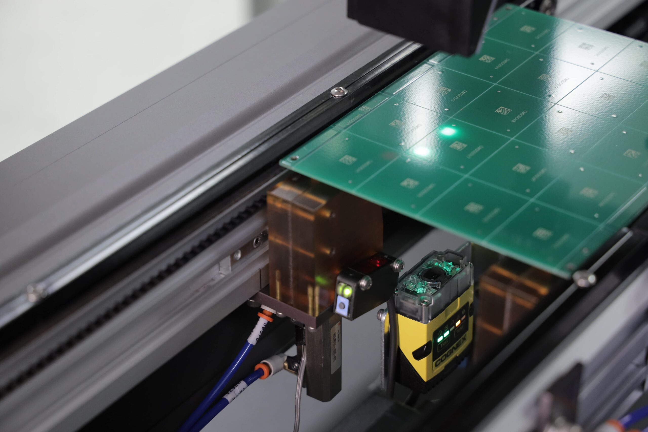
Laser Depaneling
Laser depaneling can be performed on boards requiring high tolerances. Depaneling occurs without physical contact, with no mechanical stress, and is adaptable to cut requirements through a computer controlled process. Laser depaneling is suitable for installation in surface mount technology (SMT) lines or with board unloaders/loaders for standalone operation.
Routing:
Most PCBs are routed leaving the individual circuits connected to the panel frame by narrow tabs which are subsequently broken or snapped to singulate the circuits. Routing can take up significant panel area due to wide kerf width of a physical bit.
Laser Routing:
Laser routing provides a complete software-controlled process without reliance on any mechanical dies or blades. Laser routing can cut any shape path including curves and sharp corners. The cut kerf width can be less than 20 microns, providing exceptional accuracy.
Laser routing can be performed using either:
High-power CO2 laser (~10µm wavelength)
The CO2 laser can thermally cut through FR4, glass fibers and other rigid and flex circuit substrates at comparatively high speed but with noticeable heat effect on the edge of the cut for most substrates.
Solid-state UV laser (355nm wavelength)
The UV laser, with a considerably smaller focused spot size, ablates the panel material with significantly less heat and a narrower kerf width. However, because of lower power levels, the cutting speed is much slower than the CO2 laser and the cost/watt of UV lasers is higher than that of CO2.
In general, companies that are sensitive to char and fine debris along the cut line will employ the UV laser while users who clean the circuits after singulation can benefit from the higher speed of the CO2 laser.
Final Thoughts
Laser systems for depaneling play an integral role in the future of the PCB manufacturing industry. As demand for PCBs continue to parallel technology trends, such as wearables and Internet of Things (IoT) devices, the need for systems that increase production line speed and reduce costs for manufacturer will also continue to rise.
In our Applications Development Lab, we work with each client to determine the ideal laser and optics configuration for a manufacturing process.
In this three-part series on PCB depaneling, upcoming posts will discuss the advantages and challenges of PCB depaneling, along with the evolution of PCB depaneling with laser systems.
Contact CMS Laser to discuss laser PCB depaneling systems or visit our PCB depaneling product page to learn more.


0 comments
Leave a comment.