
Laser marking is extensively used in the semiconductor industry for ensuring traceability, maintaining quality control standards, and pre-dicing scribing. This technology presents a highly precise solution to the challenges in the semiconductor industry, guaranteeing excellent process control, durable marks, and minimal material damage.
Laser technology is used to mark wafer and chip packaging materials, including:
| Silicon (Si) | Silicon on Insulator (SOI) | Silicon Carbide (SiC) |
| Gallium Arsenide (GaAs) | Gallium Phosphide (GaP) | Indium Phosphide (InP) |
| Sapphire | Crystals | Germanium (Ge) |
| Lithium Tantalate | Photoresist | Epoxies |
| Low-K Dielectric Films | Die Attach Films (DAFs) | Silicon Dioxide (SiO₂) Films |
| Plastics | Metals | Molding Compounds |
Etching or Annealing
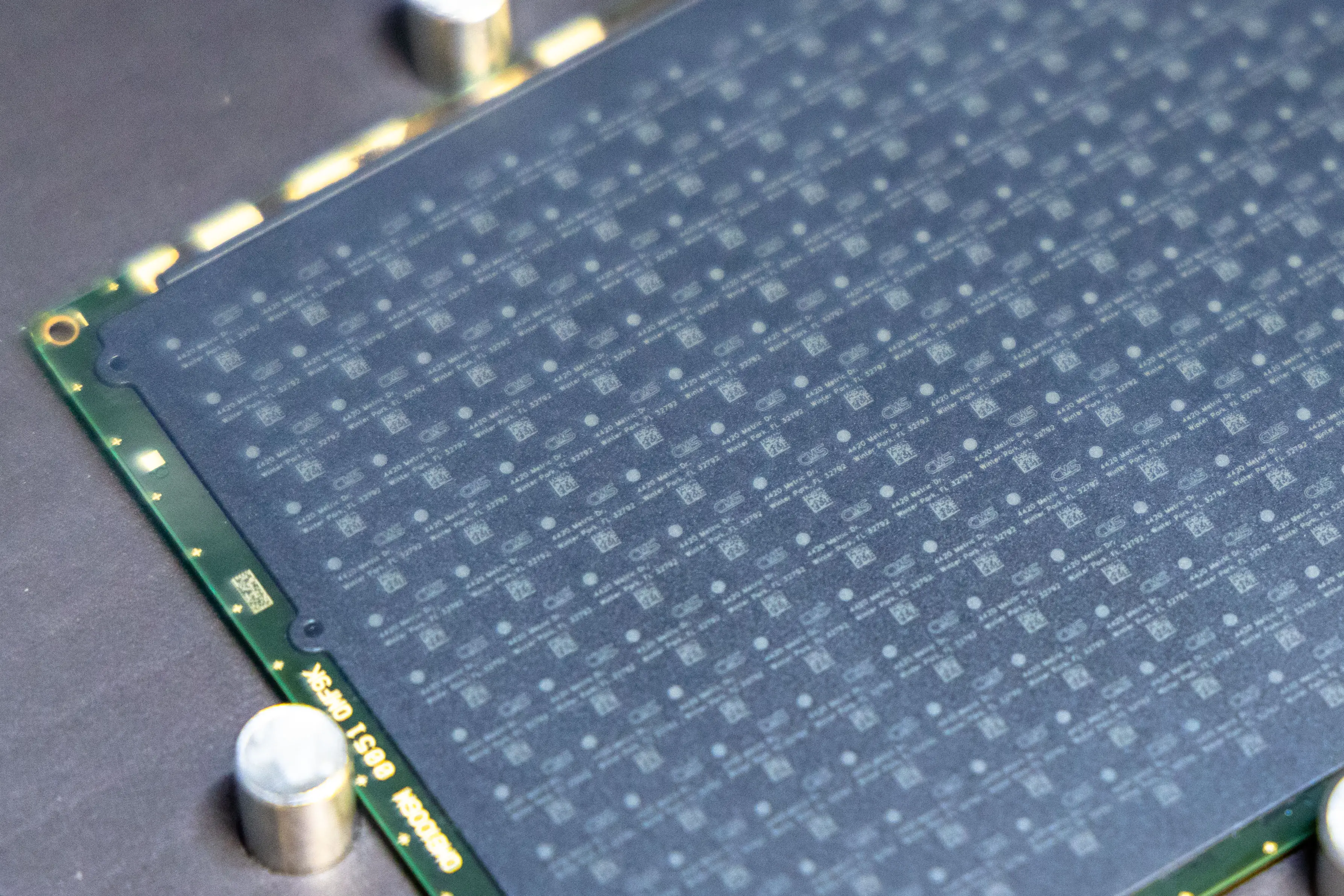
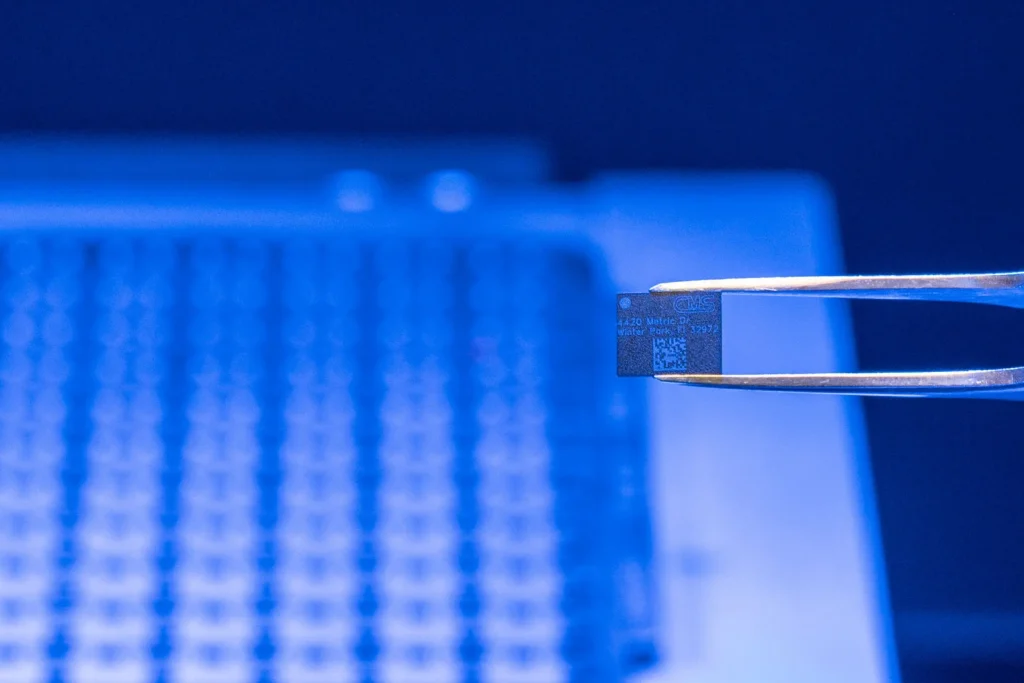
A laser beam marks surfaces through ablation or annealing – non-contact processes that produce microstructural changes with sub-micron-level detail. In ablation, or etching, laser energy is absorbed, leading to rapid heating and vaporization of the material in a pre-determined pattern, allowing for precise removal with variable depth control. Annealing, conversely, uses controlled heating below the material’s melting point to induce a change in the crystalline structure or form a thin oxide layer, resulting in a high-contrast color change without physically altering the surface.
Both processes significantly surpass alternatives like mechanical scribing and ink marking in semiconductor fabrication in terms of process tolerances, durability, reduced damage, and cleanliness.
Our System Highlights
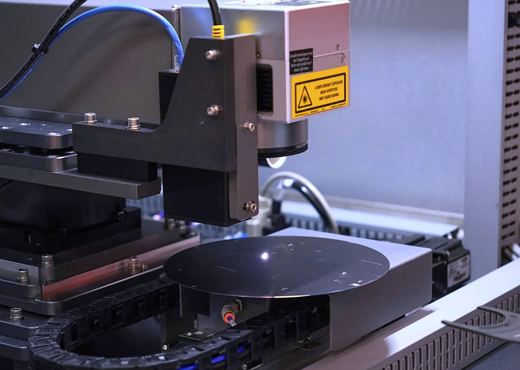
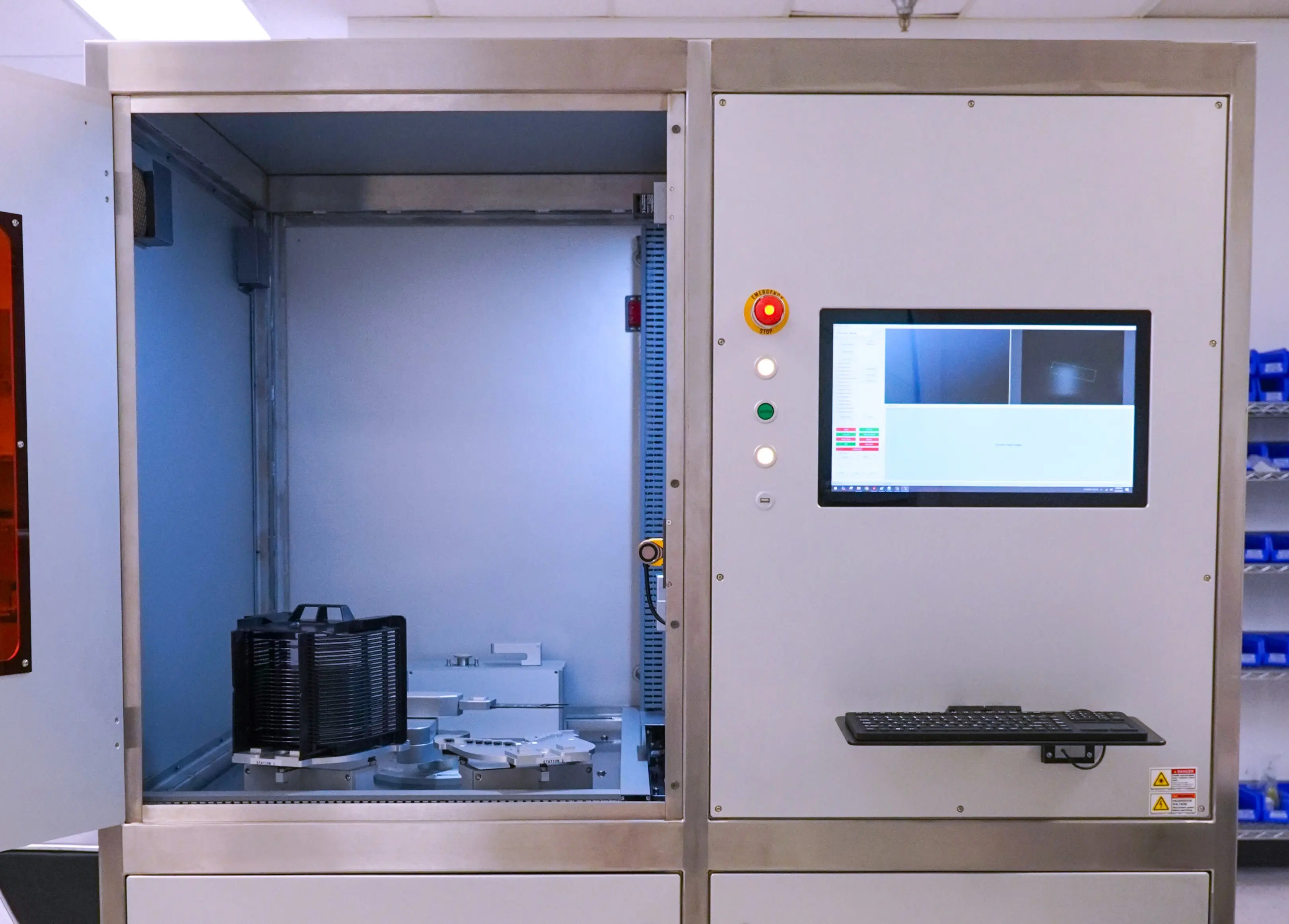
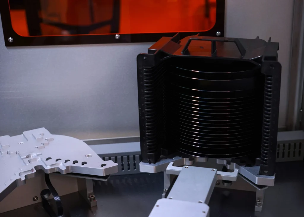
CMS Laser specializes in automated laser processing technology with proprietary software controls, delivering comprehensive laser marking systems to some of the top tech companies around the world. On our floor now a visitor can find an ytterbium fiber laser system built with a cassette-to-cassette workstation for 8-inch silicon wafers, designed to mark the backside of dies. It is complete with a flipping end-effector robot with cassette mapper for wafer transport, OCR vision technology for recognizing fiducial markers and part orientation, and a fume extractor to contain toxic particles. The wafer pre-aligner and thickness sensor ensures precise rotational and positional alignment for accurate marking.
Lastly, we tailor program controls to the needs of the client. Take advantage of the intuitive user interface that facilitates complex marking procedures, manage variable data, and connect with external databases for part numbers and automation requirements.
Click here to learn more about the automation capabilities of our turnkey industrial laser solutions.
Laser Source Selection for Required Tolerances
The types of lasers used in semiconductor wafer laser marking span across the light spectrum, from far-infrared to ultraviolet (frequency-tripled) wavelengths. The laser source you select will depend on the material processed and the tolerance requirements in your application.
- CO2 lasers offer an economical solution for serialization and dicing, particularly when larger geometries and line widths are acceptable and concerns about slag are lower. However, they can cause subsurface damage or microcracks, making them less ideal if your production deals with delicate semiconductor applications where material integrity is paramount.
- Fiber lasers – like the one currently in our assembly, this ytterbium-doped laser generates significantly less particulate than CO2 lasers, making it suitable for cleanroom environments. You’d choose this option for opaque substrates and larger feature sizes, as it can create “soft” marks on silicon with minimal debris and offers high power output with stability.
- UV lasers are preferred if process tolerances, small features, minimal slag, and reduced particulate generation are critical in your operations. The photoablation process, where small material volumes absorb high peak power UV laser energy, breaks electronic bonds, and the ejecting plasma plume carries thermal energy away, leading to minimal damage to surrounding material.
- Femtosecond lasers will get you so-called “cold marking” by eliminating thermal diffusion in a high-speed process with high pulse repetition rates. This is crucial for applications involving delicate, brittle, low-k materials on wafer topmost layers. Read more about ultrashort pulse lasers here.
Safety and Compliance
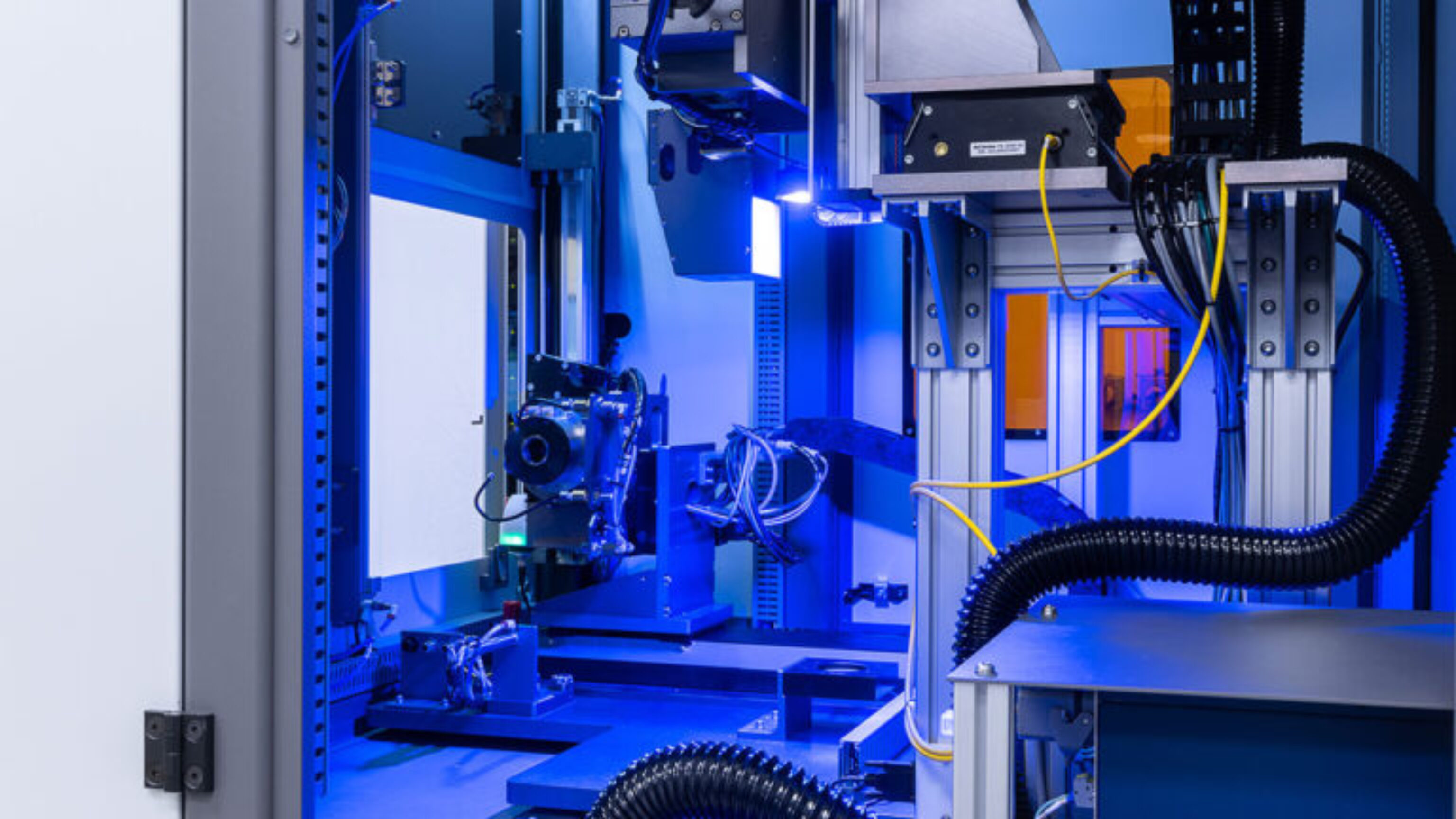
Safety standards compliance is a key aspect of CMS Laser’s systems. Our wafer marking solutions are designed to meet or exceed the safety codes of the Department of Health and Human Services, FDA for Laser Products, Center for Devices and Radiological Health (CDRH), as well as OSHA Safety Codes and the National Fire Protection Agency (NFPA) 79 Electrical Standard for Industrial Machinery. The workcell in the wafer laser marking system highlighted in this blog is enclosed in accordance with CDRH Class I standards. This prevents hazardous laser radiation and off-gassing from escaping during operation. Personnel can safely observe the process through laser-safe windows without protective gear. These systems are suitable for cleanroom manufacturing environments, including Class 10 (ISO2) cleanrooms.
Customer Service and Support
CMS Laser is committed to providing the most responsive and comprehensive customer service in the industry.
Our support begins with extensive training on the operation, care and maintenance of your laser system during your visit to our facilities for initial acceptance tests. Your training will include discreet component functionality and diagnostics to provide you with the tools to actively participate in rectifying any unforeseen system problem. After installation of your laser system, we provide technical support by phone, fax, e-mail or onsite. In most instances, we can resolve any problem within minutes of your call to our service department. If a problem cannot be resolved by phone, we can provide a service engineer onsite to quickly remedy the problem.
Immediate phone consultation with a field service engineer is available 24 hours a day. In the United States, we provide 24-hour replacement parts delivery and can typically get you onsite support within the same timeframe.
Check out our LinkedIn and Instagram pages for the latest content from current system builds and what goes into building our solutions!


0 comments
Comments for this post are closed.