
Semiconductors
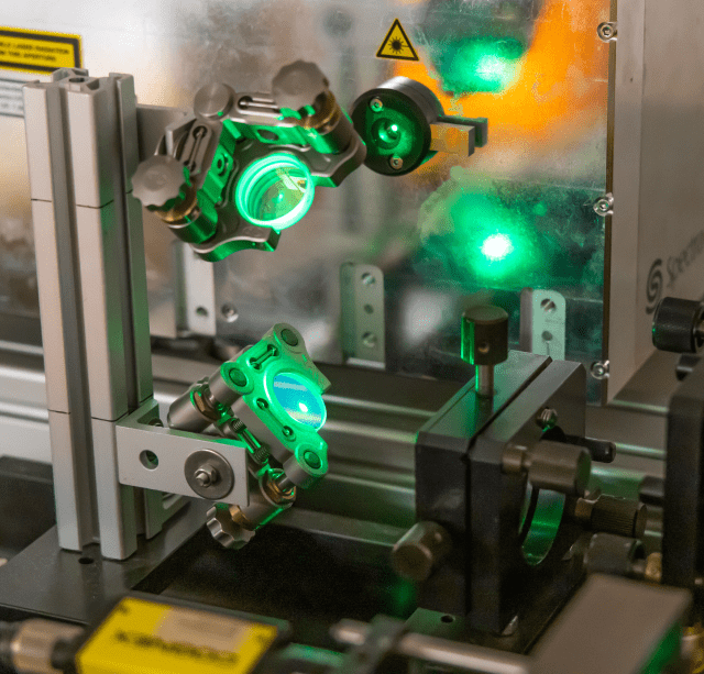
Laser material processing is a widely used technique in the semiconductor industry for marking, engraving, and scribing various compounds such as wafers, epoxies, and crystals. With the use of laser marking systems, data such as serial numbers, barcodes, and logos can be etched onto these materials to ensure traceability and maintain quality control standards.
Lasers for Semiconductors
The semiconductor wafer laser marking and engraving involves various operations such as serialization, patterning, and roughening. Choosing the appropriate laser system for these operations can be a challenging task considering the numerous process variables involved. These variables include substrate type, wafer diameter, feature size, slag tolerances, debris volume, throughput, and clean room protocols, which must all be carefully considered to ensure the best possible results.
At CMS Laser, we provide a comprehensive range of wafer laser marking and engraving solutions, including serialization for traceability, scribing, and lapping. Our laser systems are highly versatile and can process a wide variety of semiconductor substrates and coatings, such as silicon, sapphire, lithium tantalate, silicon carbide, III-V semiconductors, II-VI semiconductors, and photo resists. All our systems are designed and built in the USA.
Semiconductor Laser Applications
ULTRAVIOLET LASERS
- The UV Laser system (355nm) offers the best solution when process tolerances are the most important factor. This system allows geometries and line widths below 5 micron in dimensions and processing with minimal to no slag.
FIBER LASERS
- These systems produce less particulate than the CO2 Laser System and thus are acceptable for standard fabrication cleanrooms.
CO2 LASERS
- The CO2 Laser System offers an economical solution suitable for serialization and dicing for use in higher class cleanrooms, when larger geometries and line widths are acceptable and slag is not a major concern.
FEMTOSECOND LASERS
- New ultrafast lasers offer true “cold marking” processes and excel in areas where nanosecond lasers fail. These lasers are ideal for certain processing requirements.

- UV Laser Systems
- The UV Laser System (355nm or 266nm) is an excellent solution when process tolerances or small features are the most important deciding factor. A UV system with galvanometers and a reasonable scan field size, etches with minimal melting and microns wide line widths. This system also reduces particulate generation, especially when marking inside transparent substrates, such that it is acceptable for today’s most stringent clean room protocol.
- Fiber Laser Systems
- The Fiber Laser System (1064nm) works well with opaque substrates and larger feature sizes. With the proper laser, technique, and settings, “soft” marks (no debris) on silicon substrates are possible.
- CO2 Laser Systems
- The CO2 Laser System offers an economical solution suitable for serialization when larger line widths are acceptable and slag is not a major concern.
- Femtosecond Laser Systems
- The Femtosecond Laser System is the system of choice when true “cold marking” is required. This system is the most costly, but etchings have no raised edges or melting. Because of non-linear absorption, longer wavelengths (1040nm and 520nm) can mark transparent substrates both externally and internally. These lasers generally have high repetition frequencies that allow for faster processing.

Laser Marking Videos
UV Laser Marking System for JEDEC Tray Processing and PCB Stripmaps
View
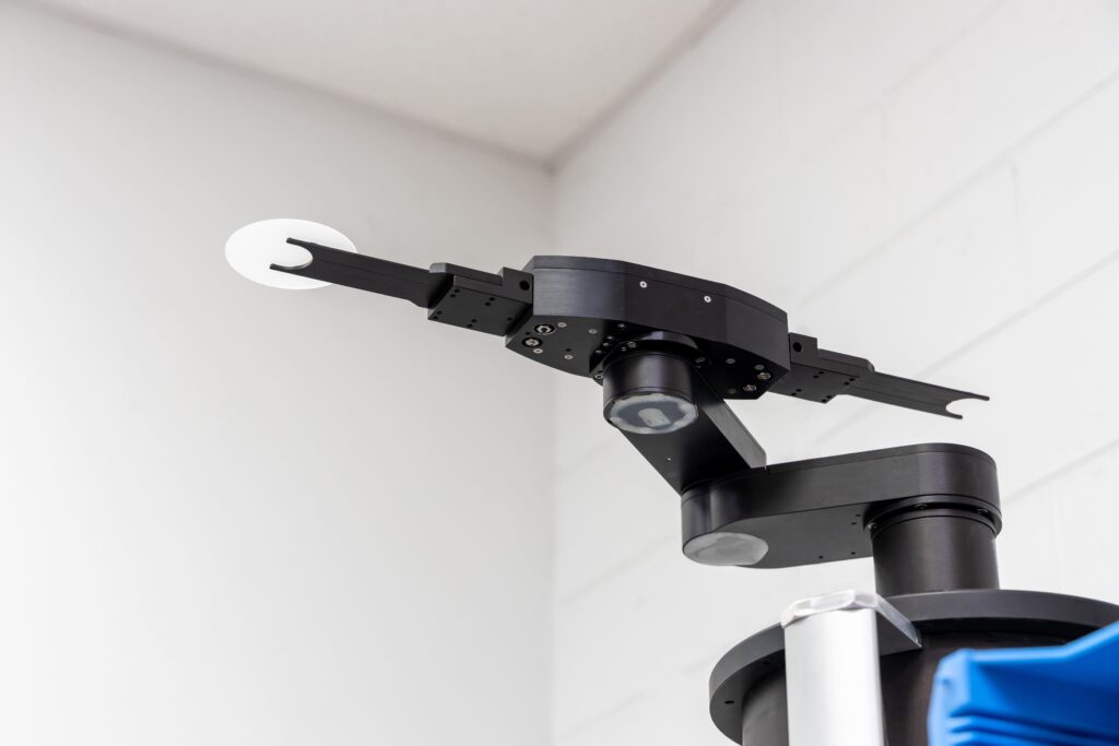
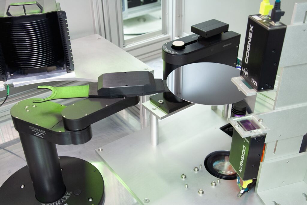
Cassette to Cassette Robotic Operation with Pre-aligner
View
Laser Marking System for Wafers using a Robot
View
Control Micro Systems Expands Laser Applications Lab Capabilities
The Absolute Best Customer Service Around
Working with the entire Control Micro Systems team on our project was a pleasure. CMS was capable of meeting and exceeding our goals. They successfully designed and built a machine which increased our throughput by 550%! We are so glad we chose to move forward with CMS.
In the three years ACR has owned the CMS laser, it has worked flawlessly. In the few instances where ACR needed support in programming, CMS was quick to respond.
CMS have been excellent partners in the development of new, complex equipment for our business. CMS built multiple machines for us. Each machine had a different purpose, however the CMS team worked openly & honestly with us to agree on optimal solutions for each one.
Need Help Finding the Right Solution?
We partner with you to develop solutions, solve problems, and create efficiencies.